Connecting multiple tact switches on a single input pin of a microcontroller
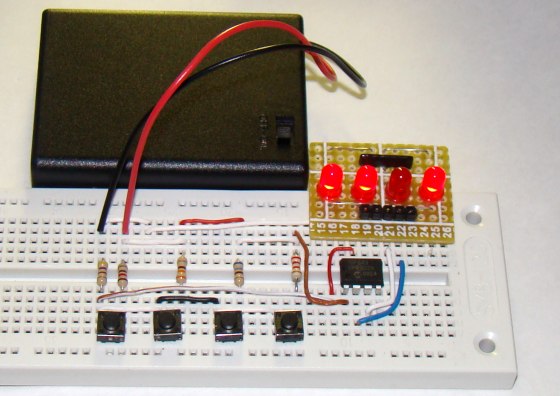
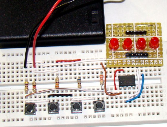
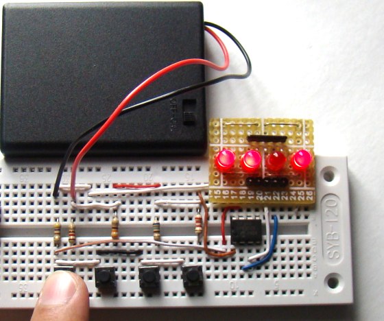
Normally one tact switch requires one digital input pin of a microcontroller. Some designs implement keypad style multiplexing to get multiple switches on fewer inputs. However, there exist other techniques that allow you to connect many switches on a single input pin of a microcontroller. This tutorial demonstrates one such technique as applied to PIC12F683 microcontroller. In this example, there are four LEDs and four tact switches connected to the PIC12F683 microcontroller. While each LED is controlled through an individual I/O pin, the four switches are connected to one ADC input pin of the PIC12F683 microcontroller.
Theory
The theory of connecting multiple switches on a single ADC input channel is very simple. One end of each switch is connected to the power supply voltage through an individual pull-up resistor, whereas the other end is grounded through a common resistor. When a switch is pressed, it creates a voltage divider network between the power supply and ground terminals. The value of the divided voltage can be made unique for all four switches by selecting different values of pull-up resistors. The voltage is then measured with the ADC to determine which switch has been pressed.
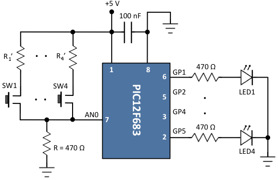
The circuit diagram shown below will probably give you a more clear picture of this technique. There are four switches (SW1-Sw4) connected to the AN0 input pin of the PIC12F683 microcontroller. Their one end is grounded through a common resistor R (=470 Ω), whereas the other end is pulled high through different value resistors (R1‘-R4‘), giving rise to different values of the voltage divider output. The voltage drop across the resistor R is thus unique for each switch press and is measured through the AN0 ADC channel. When no switch is pressed, the AN0 pin is pulled low through R, and the ADC should ideally measure 0 V.
There are four LEDs (LED1-LED4) connected to pins GP1, GP2, GP4, and GP5 of the PIC12F683 microcontroller. They will be toggled ON and OFF through the four switches.
Calculation of resistor R’
The resistors R1‘ – R4‘ determine the value of the voltage divider output for each switch press. We know that each resistor value must be different to create an unique analog voltage output across R for each switch. But how should we select their values? You should keep in mind that the resistors do have certain tolerance values and their values also change with temperature. Therefore, you should provide enough gap between any two consecutive values of the voltage divider output to avoid any conflict. The best practice would be to implement an evenly spaced values of the voltage divider for all 4 switches. Remember that when you press a switch, you should not expect a precise value of the analog voltage across the resistor R. It would fluctuate little bit within a certain range which is defined by the resistors’ tolerance values, temperature, contact resistance of the switches, and the stability of the power supply voltage. So, in order to identify the switch, what you are actually looking at is a range of voltage that the voltage divider output falls in.
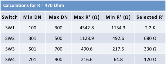
The table below shows the ranges of DN defined for all four switches, and the corresponding values for resistor R’. DN stands for digital number and represents the 10-bit A/D conversion output, which is proportional to the input analog voltage. Suppose, we define the DN range of switch SW1 as 100-300. Our goal is to find the appropriate value of R’ to ensure that when SW1 is pressed, the 10-bit A/D output will be always in between 100 and 300 count. The minimum value of R’ would correspond to the maximum value of the count, which is 300 for SW1. The equation to find R’ for DN = 100 is,
1024*R/(R+R’) = 100, where R = 470 Ω.
This gives, R’ = 4342.8 Ω. Similarly, for DN = 300, the value of R’ should be 1134.3 Ω. Therefore, R’= 2.2 K would be an appropriate value for SW1. The rest of the R’ values for other switches are shown in the table below.
Software
The software involves few if checks to compare the A/D output with the predefined ranges to determine the switch that has been pressed.
   ADC_Value = ADC_Read(0);
   if(ADC_Value > 700) {                     // SW4 is pressed
      LED4 = ~LED4;
     Delay_250ms();
   }
    if(ADC_Value > 500 && ADC_Value < 700) {  // SW3 is pressed
     LED3 = ~LED3;
      Delay_250ms();
   }
   if(ADC_Value > 300 && ADC_Value < 500) {  // SW2 is pressed
      LED2 = ~LED2;
     Delay_250ms();
   }
    if(ADC_Value > 100 && ADC_Value < 300) {  // SW1 is pressed
     LED1 = ~LED1;
      Delay_250ms();
   }
Download complete mikroC source code and HEX file
Note: The microcontroller runs at 4.0 MHz using its internal clock source and the MCLR is disabled.
Summary
A technique of interfacing multiple tact switches using a single ADC input pin was demonstrated using the PIC12F683 microcontroller. A digital input from four tact switches were individually read through the AN0 ADC channel and displayed it back on an LED. While this technique saves input pins and reduces the size, one downside of the design is detecting combination of switches. The calculations of R’ resistors become more complex in such a case. The resistor values must be chosen very carefully so that the voltage resulting from a switch combination is unique.
--
With Regards,
s.m.sethupathy,
sms communication,
Tanjore -1.
mobile :9944 186 173
www.questionpaperlink.co.cc
www.sethu-panguvarthagam.blogspot.com




Currently have 0 comments: