A new multi-function power supply unit for my Embedded Lab
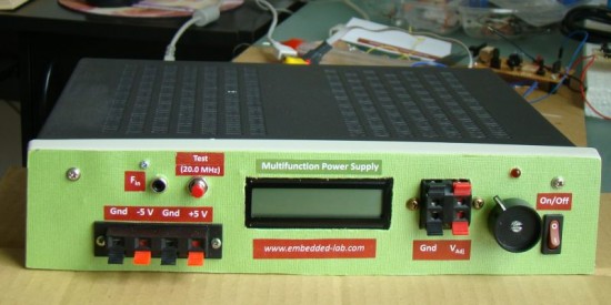
One important parameter in embedded system designing is power consumption. This parameter is directly related to the battery lifetime, if the system is to be powered from a battery. In order to determine the power rating of your designed system, you need to know how much current the system draws from the source at a given voltage. While working on my projects, I usually measure current by placing an external ammeter in series with the current's return path. This is not always convenient to do, and so I thought of making a special power supply unit for my lab that would display both voltage and current information on a LCD screen while prototyping my circuit. This way I can continuously monitor how much power my test circuit is drawing at a specific operating voltage.
This power supply unit provides fixed ±5 V as well as a variable dc voltage ranging from 1.25 V to 9 V. A PIC16F689 microcontroller is embedded into the power supply unit to measure the adjustable output voltage along with the load current. Besides, this unit also has a built-in frequency counter to measure the frequency of an external signal. The range is over 50 MHz. However, it has been tested up to 20.0 MHz, and works fine. There are still few I/O ports of PIC16F689 that are not used. So I am thinking about adding one or more features (like capacitance meter) to it. But that would be on my second version.
Theory
The fixed ±5 V power supplies are derived using LM7805 and LM7905 regulator ICs. A 12 V rectified output from a center-tapped transformer provides the dc inputs to these regulator ICs. For the variable dc output, a LM350 IC is used. LM350 is an adjustable 3-terminal positive voltage regulator that is capable of supplying in excess of 3A over a 1.2V to 33V output range. It requires only 2 external resistors to set the output voltage. Since my dc input is only 12 V (rectified output from the transformer), the regulated output from the LM350 IC would go up to 9 V (3 V less than the input, as specified in the datasheet). In order to obtain the full range of output voltage (up to 33 V) from LM350, you need a transformer with a higher output voltage. I rarely use power supply above 5 V in my projects, and therefore, a variable voltage source up to 9 V is good enough for me.
Next comes PIC16F689 microcontroller that measures the LM350 output voltage and current. You are right, I am implementing voltage and current measurement only to the LM350 output. The principles of voltage and current measurements using microcontroller were discussed in two of my posts: PIC-based digital voltmeter and How to measure dc current with a microcontroller. I am not going to repeat the details here. Both the parameters can be measured with built-in ADC channels of PIC16F689. Since the output voltage from LM350 could go higher than 5 V (up to 9 V in this situation), it is not directly measurable from an ADC channel. A simple voltage divider network using two resistors is incorporated to scale down the output voltage to the safe ADC input range (0-5 V). On the other hand, the current to be measured must be first converted into voltage so that it could me measureable too with the ADC channels. The current to voltage conversion can be done by placing a small value resistance (shunt) in series with the current path. The voltage drop across the resistance will then vary linearly with the current. I am using a 0.286 Ω resistor (Rs) made by myself by coiling a 5 ft long 22 AWG solid copper wire that has a plastic insulation on its outer surface (see the picture below).

Current sensing resistor
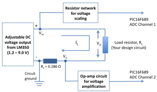
Since this resistance is so small in value, the voltage drop across won't be very high for small currents. Even for 1 A of current, the voltage drop across it would be only 0.286 V. To improve the resolution (and hence accuracy) of current measurement, this voltage must be amplified before the AD conversion process. An operational amplifier with a suitable gain can do this task. The figure below shows how this whole technique works.
An interesting thing to be noted here is that the output voltage across the load (Vo) is actually the measured voltage (Vm) minus the voltage drop across Rs (Vs). For small load current, the difference between Vm and Vo won't be very much, but it could be significant for higher current. For 1 A of load current, the output voltage across the load is 0.286 V less than the measured output voltage from LM350. This error will be corrected later in the software part by subtracting Vs from Vm.
The frequency counter uses Timer0 module in counter mode to measure the frequency of an external signal. A single transistor preamplifier stage is used to boost the low amplitude signals before they are sent to the Timer0 module for counting. An easily available BF199 RF transistor is used for this purpose.
Circuit Diagram
As mentioned earlier, two linear regulator ICs (LM7805 and LM7905) are used to derive fixed ±5 V supply. A center-tapped transformer output is rectified (using diodes) and filtered (using 4700 µF capacitors) to obtain unregulated ±12 V dc that serve as inputs to both the regulator ICs. The circuit diagram below shows all the components and their connections required for the fixed power supply.
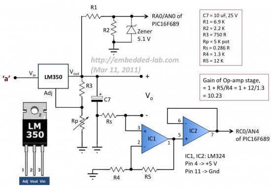
The variable power supply unit uses an adjustable regulator IC (LM350). The output voltage can be controlled through resistors R3 and Rp (see figure below). The expression for output voltage is, Vo ≈ 1.25 x (1+Rp/R3). This specific design allows the output voltage to vary from 1.25 to 9.0 V. R1 and R2 create a voltage divider network to scale the output voltage within the safe limit (0-5 V) of the microcontroller's ADC channel. An additional zener diode at the output ensures that the input voltage at PIC's ADC channel won't be greater than 5.1 V. The scaled output is connected to AN0 channel (pin 19) of PIC16F689.
The measurement of current is possible with a shunt resistor (Rs = 0.286 Ω) and an operational amplifier circuit. Rs is placed on the return path of the current and therefore, the voltage drop across it is proportional to the current drawn from the variable power source. This voltage is first amplified by a non-inverting Op-amp circuit and then passed through another non-innverting buffer stage to lower the output impedance. The output from the buffer goes to AN4 channel (pin 16) of PIC16F689 for A/D conversion. With R4 = 1.3 K and R5 = 12 K, the overall gain of Op-amp stage is 10.23. I am using LM324 IC for the Op-amp stage. LM324 does not provided rail-to-rail swing; the maximum output is about 1.5 V less than the applied power supply voltage. In this case, LM324 is powered with 0-5 V, and therefore, the maximum output voltage could be about 3.5 V. This means the maximum input voltage to the Op-amp stage would be 3.5/10.23 = 0.342 V. This gives the maximum range of the measurable current to be 0.324/0.286 = 1.2 A. Current values higher than this will saturate the LM324 output. The range of the measurable current can be increased either by decreasing the gain of the Op-amp stage or by using a different Op-amp IC that provides rail-to-rail output swing (0-5 V).
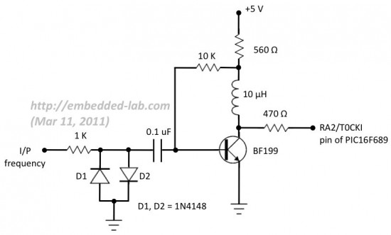
The preamplifier stage for the frequency counter has an RF transistor (BF199) that is collector-feedback biased using a 10 K resistor. The 1 K resistor with diodes D1 and D2 at the input side clamp the input signal levels to ±0.7 V. The 0.1 uF capacitor eliminates any dc component presented in the input signal. The amplified output is derived from the collector with a 470 Ω resistor in series and is sent to T0CKI pin of PIC16F689. The Timer0 module counts the number of incoming pulses through the T0CKi pin to determine the incoming frequency.
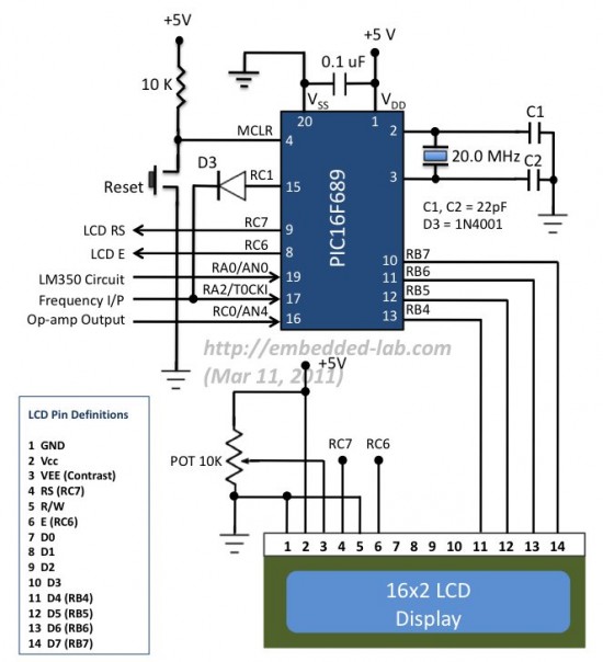
PIC16F689 runs with an external 20.0 MHz crystal. A 16 x 2 character LCD (HD44780 compatible) is interfaced in 4-bit mode. Data were transferred through RB4-RB7 pins whereas the RS and E signals are controlled through RC7 and RC6 pins, respectively. A diode connected between RC1 and RA2 acts as a gating enable for frequency counter. When RC1 is high, the T0CKI input is also held high, disabling the counting process. RC1 is set to low when the microcontroller has to count the external pulses from the preamplifier stage output. The 470 Ω resistor at the output of the preamplifier stage is to prevent any possible short circuit at T0CKI pin due to the voltage conflict between pins RC1 and RA2.
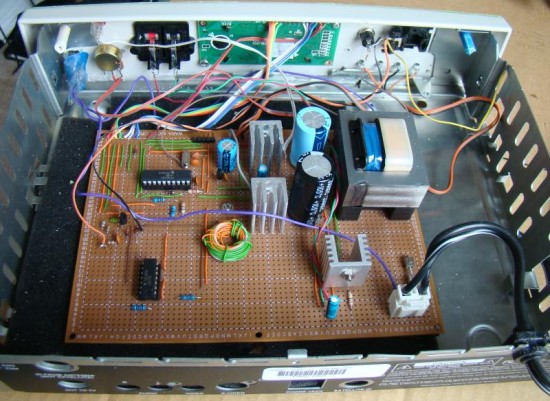
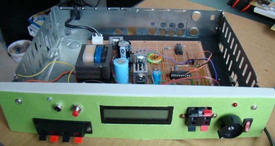
I constructed the complete circuit on a 180 mm x 128 mm general purpose prototyping circuit board which is shown below.
A/D Conversion Math
The use of A/D conversion for voltage and current measurements require some math to re-convert the digital outputs back to the voltage and current for display. Let's work on displaying the voltage first. The analog input voltage (Va) at RA0/AN0 pin is related to the A/D conversion output (digital number, DN) as,
DN = Va * (1024/5) = 204.08 * Va (Vref = 5 V, ADC resolution is 10-bit)
or, Va = 0.0049 * DN
But Va = Vout * R2/(R1+R2), Vout is the actual output from LM350.
=> Va = 0.2418*Vout
=> Vout = 4.136 * Va = 4.136 * 0.0049 * DN
=> Vout = 0.0203 * DN
This is the conversion equation for calculating the LM350 output voltage from the 10-bit A/D conversion result (DN) for channel AN0.
Similarly, for current measurement, the output of Op-amp (V0) is related to the AN4 channel A/D output as,
V0 = 0.0049 * DN (just as above)
But V0 is related to the load current (IL) through Rs as,
V0 = 10.23 * IL * Rs = 10.23 * 0.286 * IL = 2.926 * IL = 0.0049 * DN
=> IL = 0.001675 * DN (gives current from A/D conversion output)
As mentioned earlier, the output voltage is actually less than the calculated voltage (Vout) under load condition. This is because of the voltage drop across the shunt resistor Rs = 0.286 Ω due to current IL. The adjusted output voltage should be, therefore,
Vout = 0.0203 * DN – 0.286 x IL
Operation of Frequency Counter
The Timer0 module (no prescaler) is used as an external pulse counter whereas Timer1 module is used to generate a precise 100 ms duration as counting interval. This means that the resolution of frequency measurement is 10 Hz. This resolution is valid for frequencies up to 99990 Hz. Beyond this, the Timer0 module uses the prescaler (1:64) and the new resolution becomes 640 Hz or 0.64 KHz. As PIC16F689 is using 20 MHz clock, wit h 1:64 prescaler value, it can count frequencies over 50 MHz. The operation of frequency counter is like this.
- Initialize Timer1 registers with appropriate values for creating 100 ms delay.
- Enable Timer0 as counter with prescaler 1:64.
- Count the pulses for 100 ms.
- Frequency = 10 x No. of Pulses
- If frequency < 99990, change prescaler to 1:1, re-calculate frequency, and display it (in Hz). Otherwise, display the frequency in KHz.
Software
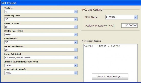
I used MikroC compiler to develop the firmware. The compiler has built-in library routines for A/D conversion, LCD display, and Timer operation. This makes the firmware development easier and quicker. Both the source code and HEX files can be downloaded from the link provided below. Configuration bits for PIC16F689 can be set using the project edit window in MikroC editor (shown below).
Download complete project source and compiled HEX files
Testing
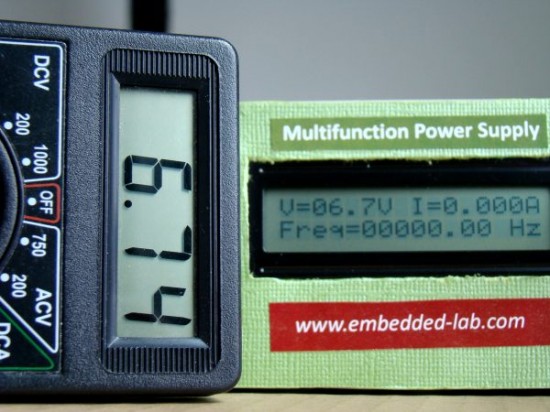
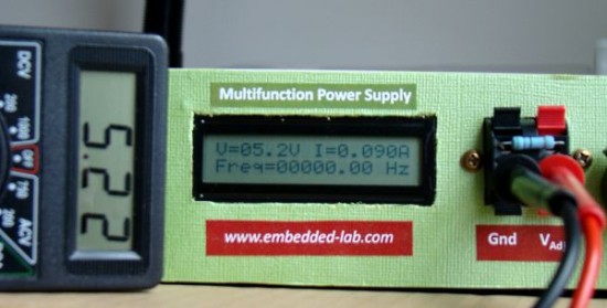
The finished project is tested for voltage, current, and frequency measurement. The displayed voltage is cross-checked with an external voltmeter, and the readings are found consistent. A 56Ω resistor is connected as load to measure current. The output voltage is set to 5.2 V, and the displayed current is 90 mA. The ideal value of current should be 5.2/56 = 92.8 mA. This gives an error of about 3% in the measurement of current but the 56 Ω resistor itself has tolerance of 5%. The testing frequency counter is done by applying the 20 MHz microcontroller clock derived from OSC2/CLKOUT pin (3). The displayed value is 20.00128 MHz which is really close.
--
With Regards,
s.m.sethupathy,
sms communication,
Tanjore -1.
mobile :9944 186 173
www.questionpaperlink.co.cc
www.sethu-panguvarthagam.blogspot.com






Currently have 0 comments: