


Testing Transistors
, Posted by ADMIN at 3:34 AM
Testing Transistors
Fig 4.1. Two Junction Transistor Model.
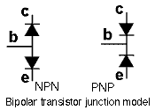
A bipolar transistor has two junctions, which can be considered simply as two diodes for our testing purposes. The "diodes" are connected back to back with their centre point being the base connection. To test a transistor you just need to check the forward and reverse resistance of both junctions, which should measure about 500 to 1K ohms in the forward direction and infinity when they are reverse biased. To do this it is neccesary to first find out which pin is which.
Use the Manufacturer´s Information
The best way to check the functions of the individual transistor pins is to use the manufacturer´s information. If a circuit diagram is available for the circuit containing the transistor, it will most probably include a "layout diagram" showing what the circuit board looks like. The connecting pins of the transistors are often identified on this drawing. Another way manufacturers use to illustrate pin−outs is a separate diagram showing the pin connections for each semiconductor used in the equipment.
Refer To A Supplier´s Catalogue
What happens if you have no manufacturer´s information? Next best is to refer to a supplier´s catalogue, and using the number stamped on the device itself, look up the data for that device, which will usually include the "package type". This is given as a number referring to a standard package with a standard layout of pins. The semiconductor section of the catalogue will normally have at least one page devoted to drawings of transistor pin−out diagrams. There are many supplier´s catalogues now on-line, most of which contain links to semiconductor data sheets. When looking for transistors or diodes these are usually listed in the "semiconductor" section. See our Links section.
Fig. 4.2. Finding the Pin Functions by Measurement.
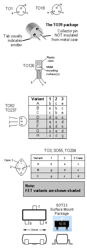
If the transistor you are testing has a metal case, such as in the TO18, TO3, TO126, TO202, TO72 etc., that is helpful. A metal case or heat sink area is almost always connected to the collector so that the heat is dissipated easier. This means that if you measure the resistance from the case to each pin in turn, the one pin that measures zero ohms is the collector. The first pin to find however must be the base. In transistor packages such as the TO18 or TO39, which both have metal cans with a small tab on the side, that´s easy. The emitter (or the source in FETs) is nearly always the connection next to the metal tab and the collector is connected to the can.
Notice that often this makes the base the centre of the three connections, but this is not always the case, as can be seen in the TO92, TO237 and SOT23 packages, don't rely on the base being at the centre. Study the common package types illustrated in Fig. 4.2. There are variations even within the same type of package. The best source for transistor pin−outs is normally a supplier´s catalogue or manufacturer´s data sheet.
If no pin−out data is available, it is still possible to identify the pins by measuring the resistance between the various pins as the next page shows. To begin with, presume that an unknown transistor may be a NPN type, as these are far more common than PNP in modern circuits.


Currently have 0 comments: